One Step Ahead

Ready to face the challenges of semiconductor miniaturization, 3D modelling and cost-cutting. In January 2022, EBARA has delivered 3,000 cumulative CMP systems.

R&D

We invest heavily in Europe to expand our leading-edge technologies such as 3-D modelling. We are prepared for the future.

Disruptive

We engage in technologies such as IoT, Car, A/R, clouds, 5G and in innovative materials such as GaN, SIC and Saphire.

Enhancing

We constantly work on new technologies for CMP tools such as polishing and plating on 6‘‘ to 12‘‘ wafers.

Efficiency

Challenge in miniaturization

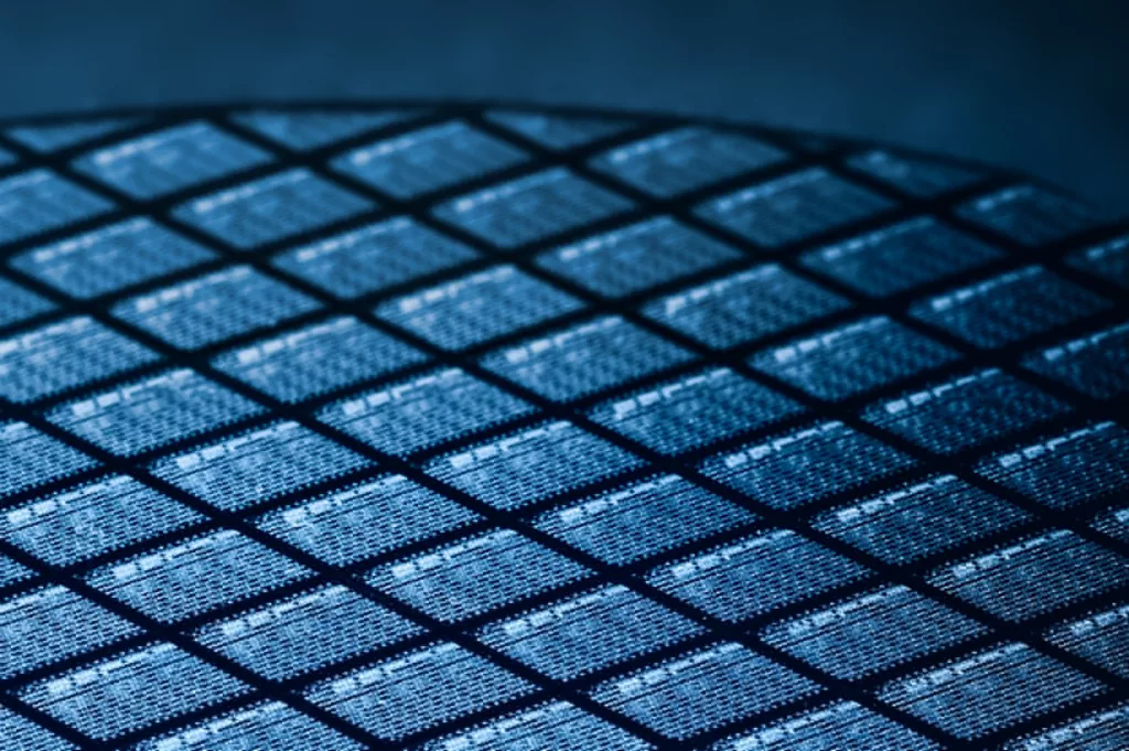
EBARA’s CMP systems enable 300-millimeter semiconductor
wafers to be miniaturized and made ultra-smooth, down
to the 10- to 20-nanometer level.

More information

Experience

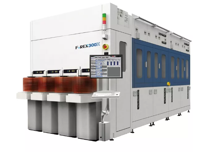
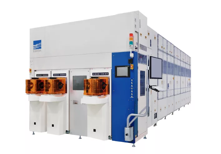
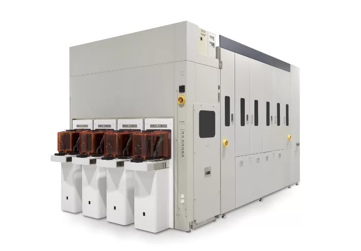
EBARA offers 4 platen platforms for CMP Systems since 2003

High flexibility and keeping the advance end point over the years by following the Moore law, EBARA stands for best solutions.

More information

Are you looking for a CMP solution?